PCBs in China are dirt cheap. There’s no doubt about that. However, sometimes I’d like to have PCB right away and I also like to challenge myself in mastering technologies. That’s probably why I occasionally experiment with a DIY fabrication of PCBs. I have a nice workflow, where I can make 6/6 mil double-sided PCBs under 45 minutes of time and roughly 15 minutes of work. There’s however one limitation – my vias are soldered through-hole wires.
I’ve been thinking about though hole plating for several years. The general procedure is simple – you have to activate non-copper surfaces (make them conductive) and then you apply standard electroplating procedure. You can find many tutorials on the internet, however, most of the require hard-to-get chemicals for the activation solution. Few weeks ago, I noticed that the local electronic component supplier had started to sell Kontakt Chemie Graphit – a conductive paint. It’s basically a colloidal graphite in an organic solution. It is supposed to be used for making surfaces conductive to prevent static electricity discharges. This could be perfect for activation of the non-copper surfaces! So I gathered all the necesery chemicals and equipment and made a test run.

First of all I took a left-over piece of double sided copper clad and drill as many holes as possible in it. I drilled holes of diameters 0.3, 0.4, …, 1.3 mm, 2 mm, 3 mm, 4 mm and 8 mm. All the drilling was piece of cake; however I got only 3 0.3mm holes as I broke my drill bit. The drill bits were no-name Chineese ones for 1.89$.
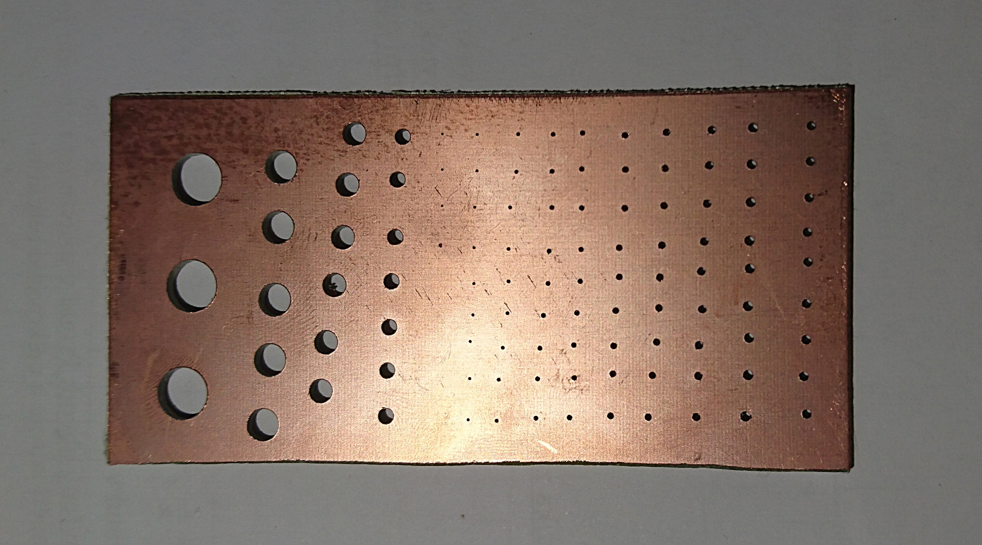


Then I wet sanded the copper with 1000 paper to polish it and remove the oxidised layer. Then I cleaned the clad in acetone to remove all the leftover dirt and fat. To activate the surface of holes, we need to cover them with the graphite spray. To do that, I sprayed thick layer of graphite and quickly sucked it to the others side via vacuum cleaner. Then I repeated the process on the other side. This leaves almost all the surface covered in graphite. Just to be sure, I cured the graphite paint at 100°C for 20 minutes. After curing I checked the resistance between the layers. I got 21 Ohms.


So far easy. I thought the next step would be challenging – we have to remove the graphite paint from the surface of the PCB, but we have to preserve conductive contact between the edge of a copper foil and the thing graphite film inside a hole. To do that I again gently wet sanded the clad with 1000 sand paper. I put the paper on a small brick with a flat edge. This ensures that I always sand in a plane and I don’t penetrate the film inside the holes. It was really easy to, as the graphite was soft. After sanding the resistance of the layers increased to 45 Ohms. During the whole process I was wearing gloves and was paying extra attention to make sure not to make the board dirty – I couldn’t clean it anymore with acetone, as it dissolves the graphite coating.
To finish the process I setup a standard acidic electroplating bath:
- 1000 millilitres of destilled water
- 160 grams of copper sulphate
- 250 millilitres of 38% sulphate acid (car battery acid)
- 2 milliliters of polysorbate 20 (to reduce the surface tension)
I put it in a round plastic container with a sufficient height. The container can be enclosed by a lid in order to make storing easier. I put the 0.1mm sheets of copper brass at the sides as anodes. Using copper electrodes ensures the solution is continuously refreshing and can be used many times (the electrodes dissolve during the process). Using the flat electrodes on both sides should give even coating. I hang my board in the middle. To secure it in place a soldered piece of copper wire.

I was electroplating for 90 minutes with a 0.8 amps, which should yield in 17 micrometer coating. I did not wanted to go with higher currents as I was afraid of getting “spongy” surface due to the evolving gases on the electrode. After 30 second I could clearly see a copper layer forming inside the holes – hurray! When the process finished, I rinsed the board. There was a dim layer of copper all over the clad. The coating was nice and even during the whole process, however, I put a wooden stick in the bath for the last 10 minutes and it yielded a dark spots on the surface. I shouldn’t repeat the mistake again. However, after polishing the surface with a sand paper I got nice, shiny surface.
Then I cut slots on one side with an exacto knife to separate the vias. Then I tested them. I used multimeter to measure the resistance. During short-circuit the multimeter with the leads show resistance of 0.1 Ohms. It was a pleasant surprise, when all the vias, except the 0.3 mm ones, reported resistance of 0.1 Ohms. Not a single defect! The 0.3 mm vias were not coated. I could see two reasons for that: either I didn’t penetrate them with the graphite coating or the surface tension was still strong and there was a trapped air buble inside the hole during the plating process. Hard to say which one was it. Next time, I try to take precautions to eliminate both effects.


After first successful test, I continued with more tests. I tried to coat them with solder. I used a standard flux. Even the surface of the holes is still dim, they coat with solder nicely. Then I tried to fill them with solder. All the sizes from 0.3 to 1.3 millimetres sucked the solder to other side nicely – just like the PCB manufactured by pros. When I soldered a pin header to the hole and rip it of, I could nicely see the cylinder filled with solder covered by the copper from the hole. Again – just like you do it on a pro board.


Overall I am surprised with the results. It just works and could be possibly used to manufacture 6/6 mill boards with 0.4 mm vias. The process is also quite simple and does not require any spacial equipment. Next time I’d like to try higher currents and I am also going to look for bath additive, which would yield in high-polish surface finish just after taking out of the bath.
As bottom line – I am not going to start make all my PCBs at home. I don’t think it is worth it in 95 % of the cases. I tried this experiment for fun and for educational purposes.
Recent news: My open letter to the 3D-printing community
I love the 3D-printing community, but I think there is room for improvement. Let's get better in 2023! Read the full letter.
Support my work!
If you like my work (these blog posts, my software and CAD models) and you would like to see more posts on various topics coming, consider supporting me in various ways:
- You can become my sponsor on Github.
- If you prefer, you can also become my Patreon.
- You can buy me a coffee on Ko-fi,
- or you can buy something from my Tindie store (also see below),
- Or you can just share my work!
If you are interested in knowing what I am up to and recent sneak-peaks, consider following me on social media (Twitter, Instagram, Facebook).
My store offers
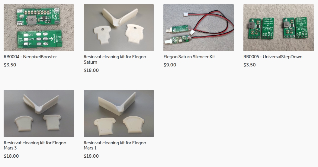
I launched new tank cleaning kits for Elegoo Saturn, Saturn S, Mars 1, and Mars 3. You can find them in my store.
Wow, just unbelievable! It opens the new horizon for prototyping, and after applying UV solder mask to PCB you could see how it will look without ordering it. Yeah, you could see similar thing in 3D view, but it’s slightly other. And sure, that way is just for prototyping, otherwise ordering PCB will be more appropriate.
How much spray did you used, by the way?
The spray formed drops when I applied it. I applied much thicker layer than you would normally applied – the spray dries out quickly and it is undesirable. The resulting layer is however quite thin as you suck most of the paint with a vacuum cleaner.
Great work! What voltage/battery was used for the electroplating?
I used a lab power supply.
what voltage is there?
Voltage doesn’t matter. You aim for constant current. Based on the temperature and the concentration of the solution my voltage was about 10-20 volts.
I’ve had luck with electroplating using just tap water and copper sulfate. What is the reason that you used battery acid as well?
Great post. I’ve been looking for a way to electroplate over plastic for a while and it looks like this might be the way.
Hey, thanks for your post on through hole plating – very interesting.
I was hoping you could make a post about how you get 6/6mil track and space? I’ve been working on my process for a while now: laser print on tracing paper, use a cnc mill to pre drill all holes, uv exposure on sensitized double sided blanks for 6 minutes, 10 minutes in hot bubbling ferric chloride. I can get 0.25mm track and space but I will have to repair a few tracks on a big board. 0.3mm track and space is what I use for reliability.
Cheers,
Matt
If all the holes including 0.3mm wicked the solder through, did that make those smallest vias conductive ? Perhaps there was enough copper in the hole to attract the solder but not make a complete surface without solder too.
The solder was wicked only on already plated boards. FR4 repels molten solder.
Hello Jan.
Please share with us also the settings from the power source. What voltages and currents did you applied?
Thanks for sharing!
As I specified in the article – you have to use constant current source. I used 0.8 for 10x5cm board
This worked for me, and I’m glad someone else figured out the chemistry for me. That said, I ended up with a rough hole and strange beading on my test board copper clad. Will it work? Absolutely. It’s electrically common and I plan to laminate my pre-etched board before trying to plate the vias. Am I curious why this happened? Absolutely.
https://imgur.com/a/UgLcN
https://imgur.com/a/Pbuu1
Thanks for the article!
Nice to hear that someone was able to reproduce my results!
I see you got really “bubbly” surface – how much current per surface area did you use? I was also thinking about stirring the bath to get more even surface, however I haven’t tried that yet.
Where to buy the conductive ink? Any links?
I don’t know where you are located, but when I enter the name of the ink, you’ll find it every – e.g. on Farnell: https://uk.farnell.com/kontakt-chemie/graphit-33-200ml/coating-conductive-200ml/dp/832959
Hello Jan!
I’m trying to reproduce your success, because that would make my life much easier, and my boards really good.
My boards currently look like this:
https://drive.google.com/file/d/1kG2_OHyMSVJZe-dx2EZyTLkmTg0Rmcxt/view?usp=sharing
What do you do to remove small air bubbles from holes? I made a electroplating bath with your recipe, but even with polysorbate there are some bubbles still in the hole.
Can you share your CNC workflow?
I assume something like this:
1. CNC -> drill holes
2. acetone ?
3. graphit
4. drying
5. sandpaper
6. electroplating
7. sandpaper
8. CNC -> top layer
9. UV mask & cure
10. CNC -> remove mask from top pads
11. CNC -> bottom layer
12. UV mask & cure bottom
13. CNC -> remove mask from bottom pads
14. CNC -> cutout
done.
What do you think ?
Thank you for sharing your idea! It’s great!!!
Hi Honza,
I tested your idea. I used content of Graphite 33 disolved in aceton and aplicated to a hole individually (in my case 0.9mm), used low preasure compresor.
Thicknes and conductivity is OK. I used copper galvanization bath with brightener (baught from FUNCHEM, Liberec), but that hole isn’t fully pleated in its height. Could it be reason I’m not using polysorbate 20. Could I try alcohol or isopropylalcohol?
I’m using both DC current 0.8A/dm2 and also pulsing reverse current 20/1 ms with anode/cathode 2:1 and 3:1 with similar result.
I can speak Czech, we could discuss it in more details if you agree.
Regards
Hi Jan, this is a great and meaningful review.
I am very grateful to you. I tried to use the laser printer toner. It works. Thank you.